Polarization induced two-dimensional confinement of carriers in wedge shaped polar semiconductors
With increasing need for high-speed electronic devices, it is necessary to enhance carrier mobility in the electronic devices. Two-dimensional electron gas (2DEG) produces a high mobility as by limiting the spatial region of occupancy, the rate of scattering from point and extended defects, which limit mobility, is minimized. Conventionally 2DEG is generated by fabricating a heterostructure of materials with different band-structures which is a complicated process. We have devised a way to generate 2DEG by growing GaN material with a particular morphology using plasma assisted molecular beam epitaxy. GaN grown along its polar axis generates polarization induced bound charges on its surface. A wedge-shaped morphology leads to a Coulombic repulsion of itinerant carriers from bounding surfaces of the wedge, confining the carriers to the center. As such, wedge shaped nanowall network shows a very high carrier mobility of up to 104 cm2/Vs. The nanoscale width of the nanowalls also causes quantum mechanical effects such as quantum confinement induced blue shift of the bandgap and quantum interference induced localization phenomenon. The GaN nanowall material has proven to be a very interesting material for fundamental and practical reasons.
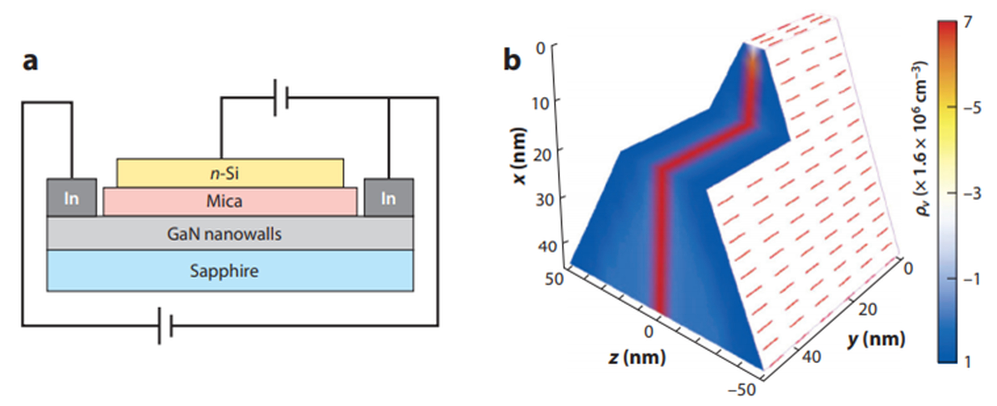
(a) Design of the field effect transistor device used for the estimation of mobility through the nanowalls. (b) Three-dimensional color plot for the charge density ρv(x, y, z) distribution inside the wedge-shaped c-oriented GaN wall. Negative and positive regions are represented by red and blue, respectively. Evidently, electrons are confined in a thin sheet located at the central vertical plane of the wall. A portion of the wall has been artificially cut open to better visualize the extent of the electron-rich central plane.
Deb, S., Bhasker, H. P., Thakur, V., Shivaprasad, S. M., & Dhar, S. (2016). Polarization induced two dimensional confinement of carriers in wedge shaped polar semiconductors. Scientific reports, 6(1), 1-7.